Test Modal

Ullenda voluptaspe natem. Ceped quam rem. Nemped que porehen ihilitatis quas endest etur alis as id quatium expelic imoluptatur repe dendere ribus, sam nonserferum nessit que vel maxim re porro od quam dolo dusaectore aperuptae qui volore, comnisquo tem incto blacepu digniet pra dit labo. Tis aspid et everfer ovidestis derro tem sedis eicabo. Optaspe rferia volesenes erro quam, sitatus solut quiatum res same atem hitiam vento is videbit velit deror autatem.
Test Modal

Ullenda voluptaspe natem. Ceped quam rem. Nemped que porehen ihilitatis quas endest etur alis as id quatium expelic imoluptatur repe dendere ribus, sam nonserferum nessit que vel maxim re porro od quam dolo dusaectore aperuptae qui volore, comnisquo tem incto blacepu digniet pra dit labo. Tis aspid et everfer ovidestis derro tem sedis eicabo. Optaspe rferia volesenes erro quam, sitatus solut quiatum res same atem hitiam vento is videbit velit deror autatem.
Test Modal

Ullenda voluptaspe natem. Ceped quam rem. Nemped que porehen ihilitatis quas endest etur alis as id quatium expelic imoluptatur repe dendere ribus, sam nonserferum nessit que vel maxim re porro od quam dolo dusaectore aperuptae qui volore, comnisquo tem incto blacepu digniet pra dit labo. Tis aspid et everfer ovidestis derro tem sedis eicabo. Optaspe rferia volesenes erro quam, sitatus solut quiatum res same atem hitiam vento is videbit velit deror autatem.

Advanced Packaging
Wafer, chip and panel level processing
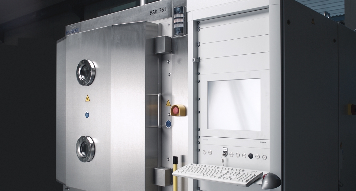
Evatec provides PVD solutions that are tailored to the various packaging platforms in the Advanced Packaging market. They combine best in class cost of ownership with unique technology innovations to meet up with todays and future requirements.
Evatec's wafer platforms that process up to 300mm formats feature highest levels of throughput, support the use of long life targets and are equipped with a unique degassing technology that achieves best in class contact resistance and layer uniformity performance required in WLCSP, FOWLP and 2.5D/3D devices.
FOPLP applications and next generation IC substrate technologies are supported by Evatec`s market leading CLUSTERLINE® 600 equipment platform. The design and concept of the panel based PVD equipment platform is based on the field proven wafer platform, and is capable of processing substrate sizes up to 650 x 650 mm, delivering highest levels in outgassing performance, layer adhesion and stack uniformity.
In EMI shielding of chips on a package level, Evatec offers production solutions with the step coverage, film adhesion and low process temperatures required to protect the chip effectively at high throughput. Latest developments support the highly cost efficient deposition of multilayers of soft magnetic materials used for integrated magnetics and EMI shields supporting low and high frequency applications needed to enable 5G.
You can read more about our thin film production solutions for Advanced Packaging applications in LAYERS
THE EVATEC TOOL PORTFOLIO FOR
ADVANCED PACKAGING
Whether it processes on wafer, panel of chip level, our production platforms are equipped with custom conditioning and source technologies suited for Advanced Packaging applications.
Our experts are on hand to help you find the right platforms according to your process requirements, throughput and factory integration requirements. Alternatively, click on the photo links to read more about each platform
CLUSTERLINE® 300
Semiconductor industry standard 300mm cluster platform equipped with proprietary degas, arctic etch and metallization technology for WLCSP, FOWLP and TSV offering flexible manufacturing capability.
HEXAGON
Dedicated compact high volume production platform for wafer level applications like WLCSP and FOWLP on 200mm and 300mm offering high speed processing for the lowest cost of ownership in the market.
CLUSTERLINE® 600
Market leading equipment solution for FOPLP and next generation IC substrate processing on panel sizes to to 650x650 mm integrating large area degas, etch and deposition technologies.
SOLARIS®
High performance indexing system with unique cooling capability and PentaPlus sputter sources with outstanding step coverage optimised for EMI shielding layers at low temperature.
Wafer Level Packaging - WLCSP & FOWLP
Organic passivated substrates, composite substrates such as silicon on glass or Fan-out Wafer Level Package (FOWLP) technology pose new challenges in processing UBM and RDL wafers. Evatec delivers dedicated degas, etch and metallization sources that ensure stable, low contact resistance over extended shield kit lifetimes of 30'000 wafers without any compromise in process quality and at throughputs up to 56 wafers per hour in Fan-out applications.
Degas Technology
Choose from new high pressure or atmospheric batch degasser technology processing up to 44 wafers simultaneously for effective removal of VOCs at moderate temperatures below 150C.
Etch and Metallization Technology
Evatec's latest generation of "Arctic Etch" source technology delivers enhanced pumping capability of remaining volatile components and the required temperature, particle management and cleanliness of the process environment for reliable low Rc at extended shield kit lifetimes.
Panel Level Packaging - FOPLP and Next Gen IC substrates
The industry push to reduce manufacturing costs and the need of innovative substrate technologies are driving the demand and requirements of panel based packaging technologies. Evatec delivers dedicated degas, etch and metallization solutions that provide excellent technical performance on large scale substrates.
Atmospheric batch degas, dual frequency CCP etch and state of the art deposition technologies handle highly outgassing organic or composite substrates with ease on substrate sizes up to 650x650mm. Proven process solutions include secure handling of thin substrates, high warpage allowance, high yield deposition of seed layer while maintaining low substrate temperature and low particle generation.
2.5D / 3D Heterogenous Integration
Vertical interconnects are considered the key elements to enable 2.5D and 3D applications. Best possible conformal step coverage of vias are supported by different technology elements from Evatec and are tailored to different via dimensions. Evatec's Highly Ionised Sputter (HIS) source technology enables deposition of metal barrier and copper seed layers at high deposition rate and long target life in aspect ratios of up to 20:1.
EMI Shielding- Package Level Processes
Evatec's SOLARIS® inline sputter platforms deliver deposition of soft magnetics and metal stacks e.g. Cu, Au, St Steel and Ti with outstanding step coverage using Evatec's Penta Plus source technology. Inline architecture enables high throughput at the lowest cost of ownership.
Evatec provides PVD solutions that are tailored to the various packaging platforms in the Advanced Packaging market. They combine best in class cost of ownership with unique technology innovations to meet up with todays and future requirements.
Evatec's wafer platforms that process up to 300mm formats feature highest levels of throughput, support the use of long life targets and are equipped with a unique degassing technology that achieves best in class contact resistance and layer uniformity performance required in WLCSP, FOWLP and 2.5D/3D devices.
FOPLP applications and next generation IC substrate technologies are supported by Evatec`s market leading CLUSTERLINE® 600 equipment platform. The design and concept of the panel based PVD equipment platform is based on the field proven wafer platform, and is capable of processing substrate sizes up to 650 x 650 mm, delivering highest levels in outgassing performance, layer adhesion and stack uniformity.
In EMI shielding of chips on a package level, Evatec offers production solutions with the step coverage, film adhesion and low process temperatures required to protect the chip effectively at high throughput. Latest developments support the highly cost efficient deposition of multilayers of soft magnetic materials used for integrated magnetics and EMI shields supporting low and high frequency applications needed to enable 5G.
You can read more about our thin film production solutions for Advanced Packaging applications in LAYERS
THE EVATEC TOOL PORTFOLIO FOR
ADVANCED PACKAGING
Whether it processes on wafer, panel of chip level, our production platforms are equipped with custom conditioning and source technologies suited for Advanced Packaging applications.
Our experts are on hand to help you find the right platforms according to your process requirements, throughput and factory integration requirements. Alternatively, click on the photo links to read more about each platform
Wafer Level Packaging - WLCSP & FOWLP
Organic passivated substrates, composite substrates such as silicon on glass or Fan-out Wafer Level Package (FOWLP) technology pose new challenges in processing UBM and RDL wafers. Evatec delivers dedicated degas, etch and metallization sources that ensure stable, low contact resistance over extended shield kit lifetimes of 30'000 wafers without any compromise in process quality and at throughputs up to 56 wafers per hour in Fan-out applications.
Degas Technology
Choose from new high pressure or atmospheric batch degasser technology processing up to 44 wafers simultaneously for effective removal of VOCs at moderate temperatures below 150C.
Etch and Metallization Technology
Evatec's latest generation of "Arctic Etch" source technology delivers enhanced pumping capability of remaining volatile components and the required temperature, particle management and cleanliness of the process environment for reliable low Rc at extended shield kit lifetimes.
Panel Level Packaging - FOPLP and Next Gen IC substrates
The industry push to reduce manufacturing costs and the need of innovative substrate technologies are driving the demand and requirements of panel based packaging technologies. Evatec delivers dedicated degas, etch and metallization solutions that provide excellent technical performance on large scale substrates.
Atmospheric batch degas, dual frequency CCP etch and state of the art deposition technologies handle highly outgassing organic or composite substrates with ease on substrate sizes up to 650x650mm. Proven process solutions include secure handling of thin substrates, high warpage allowance, high yield deposition of seed layer while maintaining low substrate temperature and low particle generation.
2.5D / 3D Heterogenous Integration
Vertical interconnects are considered the key elements to enable 2.5D and 3D applications. Best possible conformal step coverage of vias are supported by different technology elements from Evatec and are tailored to different via dimensions. Evatec's Highly Ionised Sputter (HIS) source technology enables deposition of metal barrier and copper seed layers at high deposition rate and long target life in aspect ratios of up to 20:1.
EMI Shielding- Package Level Processes
Evatec's SOLARIS® inline sputter platforms deliver deposition of soft magnetics and metal stacks e.g. Cu, Au, St Steel and Ti with outstanding step coverage using Evatec's Penta Plus source technology. Inline architecture enables high throughput at the lowest cost of ownership.