
Company Overview
Who we are and what we do
Evatec - shaping the future
Evatec thin film technology, in our offices, our homes, our cars and our smart devices. We might not see them with the naked eye, but the thin films made on our machines are everywhere. Evatec technology has been shaping the world for 70 years since the foundation of the Balzers AG company in 1946 and now Evatec know-how will enable a revolution in how we live and work. The Internet of Things (IoT) offers the potential to connect 7 trillion devices across a global population of 8 billion and Evatec thin film technology will be at its heart. The devices we enable touch the lives of millions around the globe, delivering mobile communications like 5G that run faster and electronic consumer devices that use less power to save the world’s resources.
From HB LED lighting for our automobiles to Face Recognition technology for our mobile phones, designing and building the best thin film production solutions is our daily business, and the Evatec know-how gives our customers the lead across a whole range of applications in the semiconductor, optoelectronics and photonics industries. Our coating technologies enable deposition of new materials, bring advanced process control for new levels of film performance and come with innovative system engineering for the lowest production costs.
Tomorrow’s smart technologies like artificial intelligence (AI) that sense, learn and respond to their environment will make remote healthcare accessible to millions for the first time and enable autonomous driving for a safer world. All these developments call for leaps in sensing, computing and data processing, all at higher speeds and efficiencies, all in electronic packages of smaller size and weight, and Evatec is ready. A highly skilled team of scientists and engineers armed with a portfolio of 400 patents are ready to support our customers around the globe delivering production solutions for the future.
Evatec - caring about our employees, our customers, our shareholders and our world
We aim to deliver the best customer value in the industry. To do that we need the support of the best employees and shareholders. Working with stuctured, efficient processes helps us deliver quality products in a cost effective manner. We are proud to hold ISO9001 and ISO14001 certification.
To read more about our vision, mission and environmental policy click here. To read our corporate social responsibility policy click here.
To view our ISO certification in English or German you can click the following links ISO 9001 English , ISO 9001 German , ISO14001 English , ISO14001 German
Want to know more ?
To read more about Evatec production platforms, process technologies and markets please go to the individual pages of our web site or read the case studies in our LAYERS magazines.
What we make
We are here to help you
From R&D to mass production, we deliver manufacturing solutions to our customers around the globe. Using our 70 years of process know-how we support our customers with thin film processes for today and tomorrow, leveraging advanced process control technologies for the best cost of ownership.
Contact your local sales and service organization or go on the product pages to find out more.

BAK FAMILY
Flexible family of evaporators in sizes from 0.5 to 2.0 metres for R&D or mass production
CLUSTERLINE® FAMILY
Flexible family of fully automated cluster tools up to 650mm for single substrate processing.

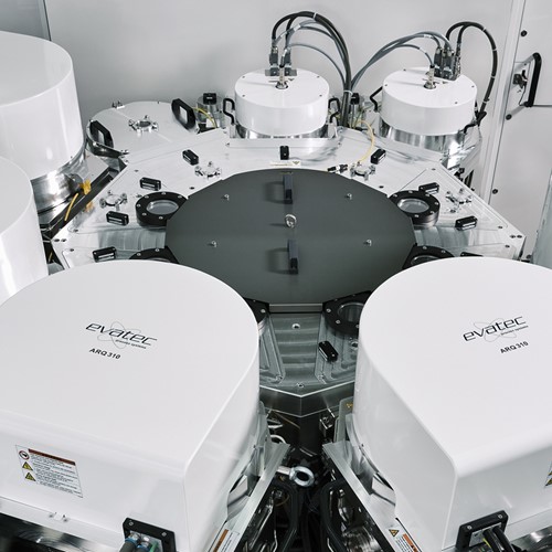
HEXAGON
Dedicated platform for wafer level advanced packaging applications like FOWLP.

LLS EVO
Vertical batch sputter platform with a proven track record in the semiconductor industry.

SOLARIS FAMILY
Family of high speed inline sputter platforms for high volume production in fully automated fabs.
Our Technology
Technology that gives you the lead
We deliver thin film process solutions (machines and processes) across Advanced Packaging, Semiconductor, Optoelectronics and Photonics using our core technology competences in etch, evaporation, sputter and PECVD technologies.
- arrow_forward Evatec’s know-how in evaporation source and process technology culminates from over 50 years experience starting with the original Balzers BAK electron beam evaporation platform. Our focus is on achieving precision at the lowest production costs through maximizing throughput and minimizing evaporation materials usage
- arrow_forward Within sputter technology we offer a whole portfolio of cathode technologies tailored to suit individual applications. Long target lifetimes / utilization combined with high transfer factors ensure best cost of ownership for our sputter processes
- arrow_forward From modification of sensitive coatings to high rate layer removal our plasma sources using technologies including ICP and CCP are powerful tools to compliment our evaporation and sputter processes
- arrow_forward Evatec's PLASMABOX® offers PECVD of high quality layers at low temperatures and low contamination when installed on CLUSTERLINE® 200 single substrate processing tools
Our Advanced Process Control (APC) technologies increase throughput, raise yields and lower cost of ownership. From control of film stoichiometry using plasma emission monitoring to precise control of layered thicknesses using quartz or optical monitoring technologies, in situ techniques across the range of Evatec production platforms deliver high performance, repeatable processes.
Evatec's Competence Laboratory (ECL)
The ECL is the place to work together with Evatec improving and developing processes for tomorrow's device technologies. At classroom levels down to ISO4, it's equipped with a suite of 30 deposition tools and over 20 measurement techniques. Click here to read more about the set up of this facility in 2019.
Want to know more?
To find out about Evatec deposition, etch and process control technologies please go to the individual technology pages of our web site or read the case studies in our LAYERS magazines.
Our Markets
Leveragign know-how across complimentary markets
Our company has a long history in supporting customers within our core markets of Advanced Packaging, Semiconductor (Power Devices, MEMS & Wireless) , Optoelectronics and Photonics. Our scientists and engineers have access to production experience and process know-how in thin film technology built up over the last 70 years.
In a world of rapid change where "semiconductor" is converging to meet "optics" we can make even greater use of that knowledge, transferring experience in one market to support developments in another. On one hand, the optical monitoring control capabilities first developed by Evatec for traditional optical film applications are now helping our customers in selected optoelectronic and semiconductor applications to achieve new levels of precision for their next generation devices. On the other hand, the fully automated wafer handling methods developed for production platforms in the semiconductor industry are now supporting our customers in emerging wafer level optics applications for optical quality layers at high yields and particle free processing.
Our markets are growing
All our markets are essential for the successful growth of the IOT. Evatec know-how in all these markets will help our customers "fast track" their technology road maps.
Want to know more?
You can read more about Evatec platforms and process capabilities in each of these markets on the various pages of our web site or within individual articles from our LAYERS magazine. Click here to contact us and request your hardcopy of our latest LAYERS magazine.