Test Modal

Ullenda voluptaspe natem. Ceped quam rem. Nemped que porehen ihilitatis quas endest etur alis as id quatium expelic imoluptatur repe dendere ribus, sam nonserferum nessit que vel maxim re porro od quam dolo dusaectore aperuptae qui volore, comnisquo tem incto blacepu digniet pra dit labo. Tis aspid et everfer ovidestis derro tem sedis eicabo. Optaspe rferia volesenes erro quam, sitatus solut quiatum res same atem hitiam vento is videbit velit deror autatem.
Test Modal

Ullenda voluptaspe natem. Ceped quam rem. Nemped que porehen ihilitatis quas endest etur alis as id quatium expelic imoluptatur repe dendere ribus, sam nonserferum nessit que vel maxim re porro od quam dolo dusaectore aperuptae qui volore, comnisquo tem incto blacepu digniet pra dit labo. Tis aspid et everfer ovidestis derro tem sedis eicabo. Optaspe rferia volesenes erro quam, sitatus solut quiatum res same atem hitiam vento is videbit velit deror autatem.
Test Modal

Ullenda voluptaspe natem. Ceped quam rem. Nemped que porehen ihilitatis quas endest etur alis as id quatium expelic imoluptatur repe dendere ribus, sam nonserferum nessit que vel maxim re porro od quam dolo dusaectore aperuptae qui volore, comnisquo tem incto blacepu digniet pra dit labo. Tis aspid et everfer ovidestis derro tem sedis eicabo. Optaspe rferia volesenes erro quam, sitatus solut quiatum res same atem hitiam vento is videbit velit deror autatem.

Optoelectronics
Solutions for LED & high performance optoelectronics
From cost effective process and production solutions for deposition of TCOs, metals and different types of DBR solutions, to AlN buffer layer deposition with highly sophisticated process control, Evatec offers a broad range of standard and customized systems. Evatec addresses the requirements for downsized future LED dimensions including passivation / protection processes (SiOX based) by optimized film uniformities,reduced particle levels and further improved process and tool stability for form factors up to 12 inch (e.g. with CLUSTERLINE® 300) and has been qualified by a number of fabs for the next generation micro LED / display technology.
Just like in LED technology Evatec can offer know-how across a number of processes in the manufacturing chain for VCSEL and EEL technologies. Evatec already has more than 15 years know-how in delivering manufacturing solutions for DBRs, TCOs, metals and passivation layers in LED applications. That know-how can be leveraged to develop tailored thin film processes for VCSEL and EEL too together with customers.
THE EVATEC TOOL PORTFOLIO FOR
OPTOELECTRONICS
We offer evaporation, sputter, PECVD and PEALD technologies on a range of batch, cluster or fully automated inline platforms.
Our experts are on hand to help you find the right platforms according to your process requirements, throughput and factory integration requirements. Alternatively, click on the photo links to read more about each platform.
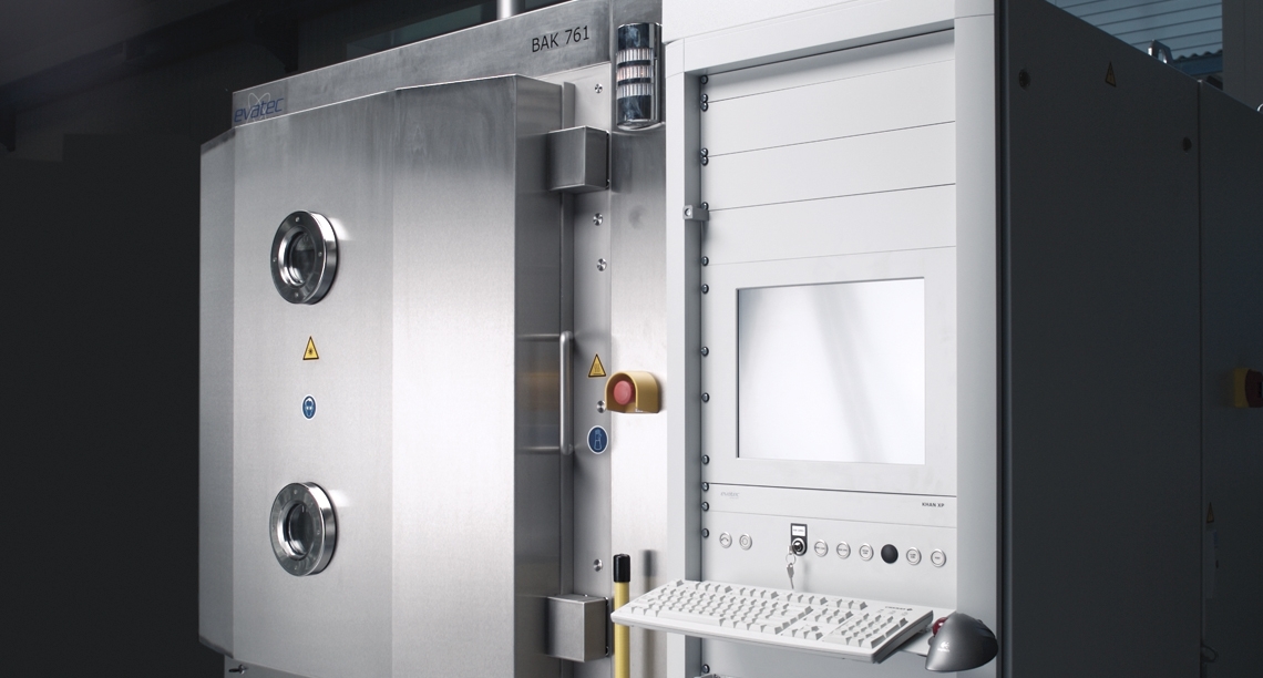
BAK FAMILY
Industry standard evaporator platforms for metals deposition and "lift off" processes. "Autoload" option for fully automated cassette to cassette production on 6 or 8 inch.
CLUSTERLINE® 200
An optoelectronics workhorse at leading LED and Micro LED Display manufacturers. Production proven for deposition processes including metals, TCOs and DBRs.
CLUSTERLINE® 300
Semiconductor industry standard cluster tool offering high uniformity deposition and etch capability on 300mm substrates and know-how for applications including OLED on CMOS.
LLS EVO II
Vertical batch sputter platform with long market pedigree the guaranteeing lowest cost of ownership especially for metal deposition.
LED Devices (Mini-, Micro- LED)
In mature LED production factors like costs of ownership plus technical drivers like LOP (light output) and forward voltage (Vf) have been dominant. For the emerging MicroLED however the focus is on other challenges right now at this relatively early stage:
- The much thinner structures make thickness uniformity across the wafer and repeatibility from wafer to wafer and batch to batch critical.
- Structures typically two orders of magnitude smaller also necessitate even better control of particles to achieve the device yields that will be required.
The lowest particle levels and best process stabilites / repeatabilities demanded for Micro LED can only be achieved in automated load lock systems. Load lock technology keeping process chambers under vacuum continuously is the best way to maintain process stability and reduce particles in continuous production, while elimination of manual handling at the front-end further reduces particles, eliminates operator handling errors and enables prefect tracking of each and every wafer through the production process.
Just like in conventional LED production, understanding the whole LED process chain is key. We know from many years experience working in close partneship with customers that the best results for overall device performance and yield come from optimizing individual processes as part of a package, but here in a nutshell are the processes where we can add value for our customers.
- TCOs ( eg ITO)
- P contacts
- N contacts
- Reflection Layers ( DBRS or metals)
- Capping layers 9 ( eg metals or SiO2)
- Finalaization ( eg low stress passivation)
At this early stage of Micro LED technology development there remain several manufacturing approaches including “mass transfer” and “monolithic” but Evatec know-how of TCO (ITO, AZO etc.), Mirror (DBR, Ag) and Metals (Ni, Ti, Pt, Au, WTi etc.) is able to support both with deposition of high transmission films across the complete visible spectrum.
You can read more about Evatec production platform and processes for Micro LED in LAYERS
Laser Diodes (VCSEL, EEL)
3D sensing technology is already well established for applications like face recognition in our mobile phones, but the technical demands for other 3D sensing in emerging applications like Autonomous Driving call for different 3D sensing technical solutions based on time of flight (TOF) with NIR VCSEL and EEL technologies. Meanwhile, other types of VCSELs like shortwave VCSEL and blue VCSEL have also drawn attention due to promising market potential in applications like datacoms, 3D printing, chip sized atomic clocks, HB light sources and so on.
Just like in LED technology Evatec can offer know-how across a number of processes in the manufacturing chain for VCSEL and EEL technologies Evatec already has more than 15 years know-how in delivering manufacturing solutions for DBRs, TCOs, metals and passivation layers in LED applications. That know-how can be leveraged to develop tailored thin film processes for VCSEL and EEL too together with customers.
Unlike LEDS, where photons may undergo only single reflection within the active region, photons may be reflected many times within the VCSEL cavity so DBR performance with very high reflectivities on both front and back sides is critical to avoid unacceptable losses in light output.
Sputtered DBR layers can potentially deliver significant device performance advantages over traditional epitaxial layers, especially in the blue domain, through:
- Higher peak reflectance for improved light output
- Wider stop band for larger wavelength range
- Lower spectral shift for improved yield
- Thinner stack structure for less surface stress
- Lower total resistance for increased efficiency
You can tead more about Evatec production platforms amnd processes for VCSEL in LAYERS
From cost effective process and production solutions for deposition of TCOs, metals and different types of DBR solutions, to AlN buffer layer deposition with highly sophisticated process control, Evatec offers a broad range of standard and customized systems. Evatec addresses the requirements for downsized future LED dimensions including passivation / protection processes (SiOX based) by optimized film uniformities,reduced particle levels and further improved process and tool stability for form factors up to 12 inch (e.g. with CLUSTERLINE® 300) and has been qualified by a number of fabs for the next generation micro LED / display technology.
Just like in LED technology Evatec can offer know-how across a number of processes in the manufacturing chain for VCSEL and EEL technologies. Evatec already has more than 15 years know-how in delivering manufacturing solutions for DBRs, TCOs, metals and passivation layers in LED applications. That know-how can be leveraged to develop tailored thin film processes for VCSEL and EEL too together with customers.
THE EVATEC TOOL PORTFOLIO FOR
OPTOELECTRONICS
We offer evaporation, sputter, PECVD and PEALD technologies on a range of batch, cluster or fully automated inline platforms.
Our experts are on hand to help you find the right platforms according to your process requirements, throughput and factory integration requirements. Alternatively, click on the photo links to read more about each platform.
LED Devices (Mini-, Micro- LED)
In mature LED production factors like costs of ownership plus technical drivers like LOP (light output) and forward voltage (Vf) have been dominant. For the emerging MicroLED however the focus is on other challenges right now at this relatively early stage:
- The much thinner structures make thickness uniformity across the wafer and repeatibility from wafer to wafer and batch to batch critical.
- Structures typically two orders of magnitude smaller also necessitate even better control of particles to achieve the device yields that will be required.
The lowest particle levels and best process stabilites / repeatabilities demanded for Micro LED can only be achieved in automated load lock systems. Load lock technology keeping process chambers under vacuum continuously is the best way to maintain process stability and reduce particles in continuous production, while elimination of manual handling at the front-end further reduces particles, eliminates operator handling errors and enables prefect tracking of each and every wafer through the production process.
Just like in conventional LED production, understanding the whole LED process chain is key. We know from many years experience working in close partneship with customers that the best results for overall device performance and yield come from optimizing individual processes as part of a package, but here in a nutshell are the processes where we can add value for our customers.
- TCOs ( eg ITO)
- P contacts
- N contacts
- Reflection Layers ( DBRS or metals)
- Capping layers 9 ( eg metals or SiO2)
- Finalaization ( eg low stress passivation)
At this early stage of Micro LED technology development there remain several manufacturing approaches including “mass transfer” and “monolithic” but Evatec know-how of TCO (ITO, AZO etc.), Mirror (DBR, Ag) and Metals (Ni, Ti, Pt, Au, WTi etc.) is able to support both with deposition of high transmission films across the complete visible spectrum.
You can read more about Evatec production platform and processes for Micro LED in LAYERS
Laser Diodes (VCSEL, EEL)
3D sensing technology is already well established for applications like face recognition in our mobile phones, but the technical demands for other 3D sensing in emerging applications like Autonomous Driving call for different 3D sensing technical solutions based on time of flight (TOF) with NIR VCSEL and EEL technologies. Meanwhile, other types of VCSELs like shortwave VCSEL and blue VCSEL have also drawn attention due to promising market potential in applications like datacoms, 3D printing, chip sized atomic clocks, HB light sources and so on.
Just like in LED technology Evatec can offer know-how across a number of processes in the manufacturing chain for VCSEL and EEL technologies Evatec already has more than 15 years know-how in delivering manufacturing solutions for DBRs, TCOs, metals and passivation layers in LED applications. That know-how can be leveraged to develop tailored thin film processes for VCSEL and EEL too together with customers.
Unlike LEDS, where photons may undergo only single reflection within the active region, photons may be reflected many times within the VCSEL cavity so DBR performance with very high reflectivities on both front and back sides is critical to avoid unacceptable losses in light output.
Sputtered DBR layers can potentially deliver significant device performance advantages over traditional epitaxial layers, especially in the blue domain, through:
- Higher peak reflectance for improved light output
- Wider stop band for larger wavelength range
- Lower spectral shift for improved yield
- Thinner stack structure for less surface stress
- Lower total resistance for increased efficiency
You can tead more about Evatec production platforms amnd processes for VCSEL in LAYERS