
Frontend
Thin film solutions for semiconductor devices with advanced nodes
Helping Customers innovate in new architectures
Enabling 3D Integration
- Stress management and wafer warpage correction
- PVD processes for Hybrid Bonding
Conformal coatings
- For various devices using multilevel interconnect architecture
- Suitable for large CD ~400-500nm down to less than 100nm
Sputtered Hard Masks
- Proven Evatec PVD process solutions
- Wide portfolio of materials and processes
Why Evatec is your partner in Frontend
The demand to build smaller/faster/more efficient devices has driven the semiconductor industry over the last decades. As progress in 2D scaling slows other approaches are needed to boost device performance.
Innovations in new materials, architectures (e.g. transistor designs) or innovations by introducing the 3rd dimension are required to further increase logic density.
Evatec sputter equipment like CLUSTERLINE® 300 for processing of 300mm wafers is available in a dedicated CMOS configuration for improved vacuum, defects and contamination performance.
Here are just some of the areas where we can support you so reach out to us in case of any queries.
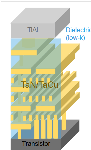
Multilevel interconnect metallization for ICs:
Interconnect metallization within integrated circuits enables signal transfer between devices. While earlier generations commonly used aluminum, the industry later adopted copper with Ta/TaN barrier layers to meet tighter design rules and reduce resistivity. Today, Evatec supports both traditional and advanced metallization needs with a dedicated CMOS-compatible CLUSTERLINE® 300 system.
Our flexible hardware configurations, including advanced temperature control through cold and hot electrostatic chucks (ESCs), ensure high process repeatability. We offer titanium-aluminum process solutions for higher-level metallization and metal pad formation in applications such as high bandwidth memory (HBM). In addition, our process team is ready to support your development of Ta/TaN barrier and Cu seed processes to meet the demands of next-generation interconnects.
Warpage Compensation
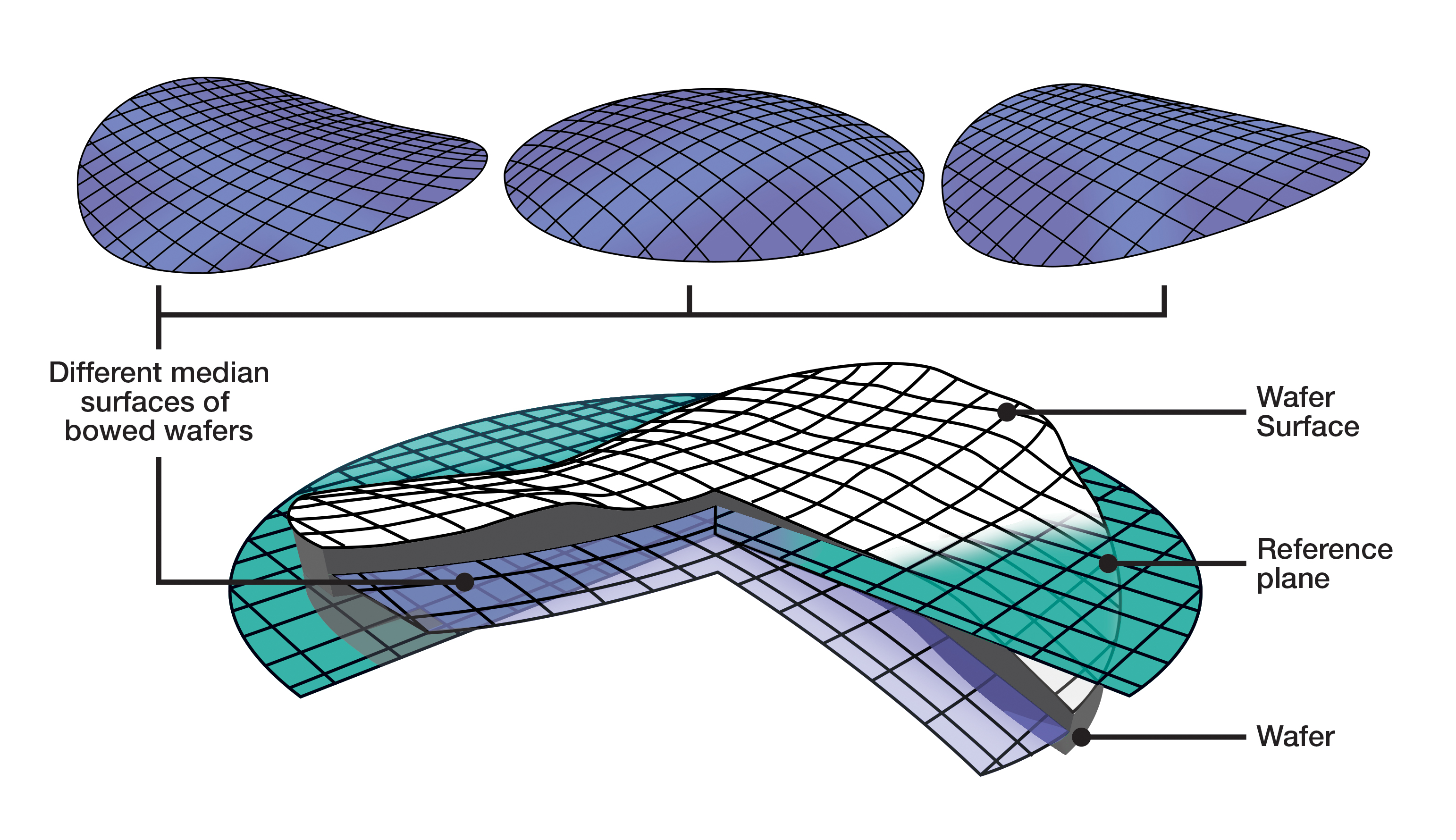
Warpage Compensation in Semiconductor Manufacturing
As semiconductor devices become more complex, vertically stacked wafers are increasingly used to achieve higher functional and storage density. One way to overcome the resulting wafer deformation and substrate warpage is backside wafer warpage correction (WPC) through a dielectric PVD layer. Using a compressive nitride PVD solution enables tunable stress films at low temperatures, preserving wafer integrity.
Key specifications for successful WPC include stress range, layer thickness, substrate temperature, edge roll-off, and chemical properties, especially for post-treatment steps such as etch removal.
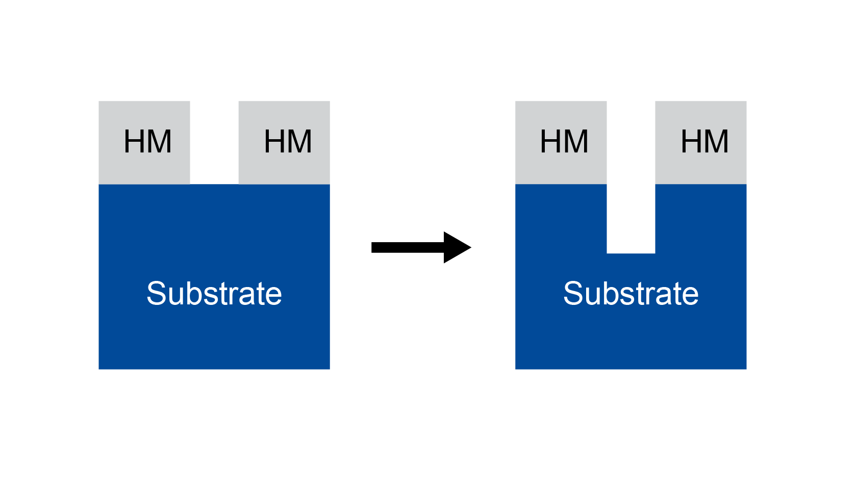
Hard Masks
Hard masks in Semiconductor Manufacturing
Hard masks play a crucial role in the manufacturing process of devices, including memories. These masks serve multiple purposes:
- Pattern Definition: Hard masks define patterns, acting as etch masks or defining implantation regions. They guide subsequent processing steps with precision.
- Etch Stop: In addition to a pattern a hard mask can act as well as a etch stop to control and limit the debt of the etch process.
- Etch Selectivity and Efficiency: Hard masks must exhibit high etch selectivity. This property ensures that during plasma etching, the mask material remains intact while the underlying layers are selectively removed. This enables the use of thinner layers and higher process throughput.
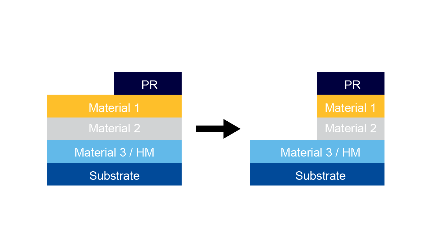
However, achieving an effective hard mask involves considering additional factors:
- check Mechanical Properties: Hard masks should withstand various stresses during fabrication, ensuring their stability and durability.
- check Deposition Technologies: Chemical vapor deposition (CVD) is widely used for hard mask deposition due to its uniform and conformal coverage. However, it may face limitations in applications with strict thermal budgets or where high hydrogen content must be managed. In such cases, physical vapor deposition (PVD) offers a viable alternative.
- check Material Options: Various compositions, such as MoO2, SiC(N), Ta2O5, and SiN, are available. Each material can be demonstrated for suitability in specific applications.
For further information or inquiries, please feel free to contact us.
Production Tools
The Evatec Tool Portfolio for Frontend:
Choose from Evatec's platforms based on your substrate, process requirements, throughput, and factory integration needs.
Our experts are available to assist you in finding the right platform tailored to your specifications. Alternatively, click on the button to explore each platform in detail.
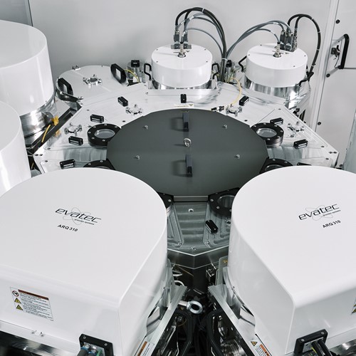
CLUSTERLINE® 300
Cluster platform architecture with single wafer processing and completely automated handling for front and back metals on 300mm wafers in volume production.
Read more about Frontend in our LAYERS magazine

Beyond Moore's Law
Chip makers face challenges in 3D IC and heterogeneous integration, needing to manage thermal budgets and wafer flatness. Evatec offers solutions for advanced CMOS fabs.