Proven production performance in panel processing
Production tools around the globe
- Panels up to 650x650mm
- Solutions for emerging panel sizes including 310x310mm
"Seed Layer" processes
- Conformal coatings for trenches and vias
- Processes for high aspect ratios
Next gen. IC Substrate and Chiplet Packages
- PVD processes reducing carbon footprint and enabling smaller structures
- Substrate flip capability for double sided processes
Industry leading production solutions
- Degas, Etch and PVD process solutions
- Lowest Rc and highest throughputs for best CoO
Fan-Out Panel-Level Packaging and Advanced IC Substrates
New types of Neural Networks, such as ChatGPT and other text generators, along with various Artificial Intelligence (AI) applications, are driving the demand for High-Performance Computing (HPC) to unprecedented levels. Innovations like Chiplet-Packages, novel Heat Dissipation methods, Miniaturization, new Material Integration, and Power Optimization showcase the vital role of Advanced Packaging for these advances.
With high adoption rates and significant technological advantages, Advanced Packaging at panel level is a rapidly growing segment providing a pathway to support industry roadmaps.
From 310x310mm to 650x650mm, innovations and opportunities in Panel Level Packaging
Sputtered seed layers, which are replacing chemical seed layers, enable a range of new possibilities. Both OEMs and manufacturers of next-generation IC Substrates and Substrate-like PCBs are adopting sputtered seed layers as an enabling technology for smaller, more precise structures, improved reliability and reduced carbon footprint for their manufacturing processes integrating new materials into packages, such as glass core with Through Glass Via (TGV), and developing next-generation Chiplet-Packages present exciting opportunities ahead.
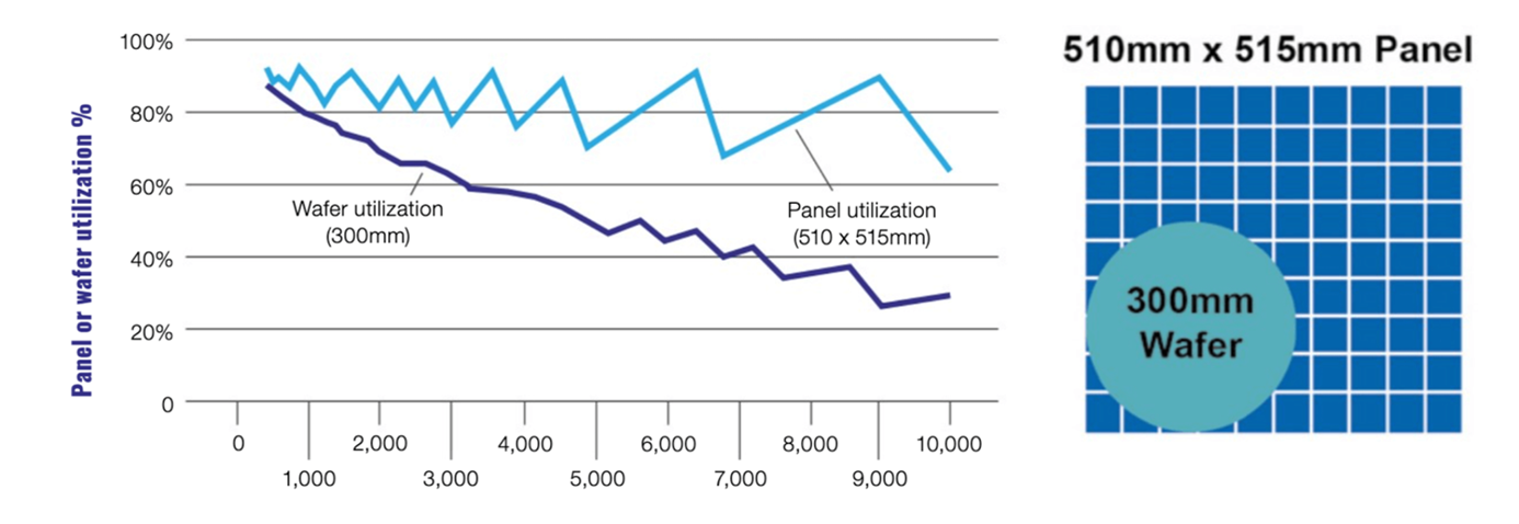
The integration of ever more Chips into a single package increases the size of these packages. As package sizes grow, material and equipment utilization on round wafers becomes inefficient. Therefore, the industry is shifting towards panel-sized semiconductor-grade process equipment, which handles and processes rectangular substrates with dimensions ranging from 300x300mm up to 600x600mm and more

Evatec is a market leader in panel-sized semiconductor-grade process equipment for Fan-Out Panel Level Packaging and Advanced IC Substrates, utilizing a variety of materials. Evatec's market-leading CLUSTERLINE® 600 platform processes substrate sizes up to 650x650mm, delivering top performance in outgassing, seed layer adhesion, and stack uniformity.
Production Tools
The Evatec Tool Portfolio for Panel Level Packaging:
Choose from Evatec's platforms based on your substrate, process requirements, throughput, and factory integration needs.
Our experts are available to assist you in finding the right platform tailored to your specifications. Alternatively, click on the button to explore each platform in detail.

CLUSTERLINE® 600
Market leading equipment solution for FOPLP and next generation IC substrate processing on panel sizes up to 650x650 mm integrating large area degas, etch and deposition technologies.
Read more about Panel Level Packaging in our LAYERS magazine

Greener PCB / IC-Substrate industry
Find out how the CO2 footprint of PCB manufacturing can be reduced by reducing raw materials and wet processes, optimizing product build
ups and introducing dry processes.

CLUSTERLINE® 600 & next generation IC-substrates
Recent advances on our CLUSTERLINE® 600 platform highlight its suitability for manufacturing advanced IC-substrates for emerging markets like AI and High Performance Computing.

Key challenges in fan-out packaging technologies
Samsung Electro-Mechanics talks about working with Evatec to solve challenges in Fan-out packaging technologies for successful production of the Samsung GALAXY watch.
