Your full service provider – Si & Wide Band Gap
50 years of know-how in Power
- Reliable thin film wafer handling
- Proven management of film stress and particles
A complete portfolio on Si
- Front and backside solutions on 200 & 300mm
- Trench filling & planarization, contacts, wetting and capping processes
Leveraging know-how on Si and more !
- Direct or bonded wafer handling
- Custom processes including Carbon Capping layers
Innovation in emerging GaN technology
- Novel PVD deposition processes
- Lattice matching / seed layers
Benefit from Evatec's long experience in Power Devices
Evatec's long experience in Power Device applications helps you optimize productivity, ensure process stability, and improve yield to drive down your production costs. We offer sputtering and evaporation tools tailored for high-volume production of power transistors like IGBT and MOSFETs, diodes, rectifiers and thyristors.
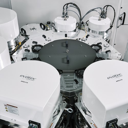
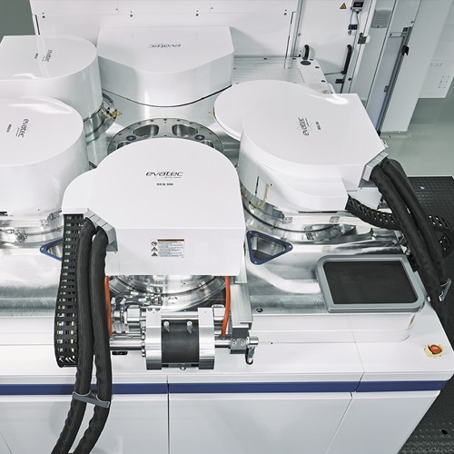
Within our sputter technology portfolio, Evatec's CLUSTERLINE® family comprises 200mm and 300mm tools tailored for high-throughput applications. Our single wafer processing modules feature high-rate sputtering sources and advanced temperature management functionalities, ensuring precise process control and superior particle performance. The cluster tool architecture of CLUSTERLINE® significantly improves process stability and productivity, rendering it well-suited for demanding applications.
For processes like Backside Metallization (BSM) on thin wafers, our CLUSTERLINE® platforms enable direct, secure processing of 200mm wafers down to 70 microns and 200/300mm Taiko wafers down to 60 microns ensuring defect-free metallization processes. CLUSTERLINE® 200 & 300 offer backside processes including in-situ pre-etch with Ar/H2, in-situ annealing, stress and temperature management, and high-quality ohmic contact formation with minimal wafer bow or warp.
Trends in frontside contact formation in new power device technologies on Si or SiC are calling for ever more demanding thin film processes. Evatec’s CLUSTERLINE® 200 offers solutions to achieve sufficient side wall and bottom coverage for trenches/vias with an aspect ratio 3:1 and higher without siginificant increase in overall film thickness.
Our evaporation solutions are based on the industry-standard BAK family, known for its flexibility and reliability. Featuring planetary handling and flip systems, these platforms excel in depositing thick frontside aluminum or backside contact stacks in single or double-sided processes.
Supporting perfect aluminium flow in higher aspect ratio trenches
Applications for Si, SiC & GaN
Frontside processes
- check Ohmic contacts
- check Surface protection for SiC
- check Trench filling including high aspcect ratio
- check Sputtered AlN seed layer for MOCVD GaN growth
- check Solderable top metal stack
- check Thick metal (Al, Cu)
Backside processes
- check Etching / surface cleaning
- check Ohmic contacts
- check Backside metal stack
- check Contactless wafer handling

SiC and GaN WBG technology
For SiC and GaN on Si applications, Evatec’s tool portfolio provides a diverse range of process technologies to facilitate high-end deposition processes for both developmental and high-volume production of demanding new device types. In addition to frontside and backside metal deposition processes, we offer sputtered amorphous carbon protection layers on SiC surfaces to mitigate high wafer roughness resulting from high-temperature annealing after ion implantation.
Contact us to learn more about our SiC and GaN WBG technology solutions including processing of thin and bonded wafers.
Production Tools
The Evatec Tool Portfolio for Power Devices
We offer a huge range of evaporation and sputter technologies on batch, cluster, or fully automated inline platforms to satisfy your needs. Click on the buttons below to learn more about each platform as a first step, then contact our experts to assist you in selecting the right platforms based on your specific process requirements, throughput needs, and factory integration criteria.

BAK Family
Flexible evaporators offering planetary handling and flip systems for deposition of thick frontside aluminium or backside contact stacks in single or double sided processes.

CLUSTERLINE® 200
Cluster platform architecture with single wafer processing and completely automated handling for front and backside metals on 150 or 200mm wafers in volume production.

CLUSTERLINE® 300
Cluster platform architecture with single wafer processing and completely automated handling for front and backside metals on 300mm wafers in volume production.

SOLARIS®
Inline production solution for cost sensitive applications for thick frontside metal, selected double sided or backside metal processes for wafer sizes up to 8 inch.

HEXAGON
As market economics get more and more tough contact us to find out how HEXAGON can double your throughput in selected backside metallization applications where process specifications allow.

LLS EVO II
Vertical batch sputter platform with long market pedigree guaranteeing lowest cost of ownership especially for metal deposition.
Read more about Power Devices in our LAYERS magazine

Advances in Frontside Process Technology
Trends in frontside contact formation in new power device technologies on Si or SiC are calling for ever more demanding thin film processes.

New Cu Frontside processes on 300mm
Find out why Evatec's CLUSTERLINE® 300 is the ideal platform to satisfy the growing demand for 300mm processing.

Low-Field Transport in n-GaN via Ga Sputtering
Experts talk about the work being done on sputtering from a liquid Ga-target.
Want to know more?
Learn more about our SiC and GaN WBG technology solutions including processing of thin and bonded wafers.
