Delivering the lowest Cost of Ownership in WLP
Enabling Heterogeneous Integration
- PVD solutions for wafer warpage correction
- SiCN hybrid bonding solutions
"Seed Layer" processes
- Precise conformal coatings
- High aspect ratio trenches and vias
High Performance Computing & AI
- Heat Dissipation applications
- Solderable layer processes
Industry leading production solutions
- Degas, Etch and PVD process solutions on 200 or 300mm
- Lowest Rc and highest throughputs for best CoO
Proven know-how in Wafer Level Packaging Processes
Choose Evatec as your partner for wafer level packaging processes secure in the knowledge that our platforms and processes are already in daily use around the globe at the world's leading packaging houses around the globe. Whether it's the broad configuration and process flexibility of our CLUSTERLINE® 300 or the applications targeted specifically by HEXAGON, you can be sure there will be a production solution that's just right for you. Evatec's wafer level platforms process formats up to 300mm feature highest levels of throughput, support the use of long life targets and are equipped with a unique degassing technology that achieves best in class contact resistance and layer uniformity performance required in WLCSP, FOWLP and 2.5D/3D devices.
Bumping (UBM)
Bumping, a crucial technique for establishing connections between chips, substrates, and PCBs, involves the creation of raised metal regions known as "bumps" over bonding pads. Evatec offers a comprehensive range of bumping solutions tailored to various applications and specifications. Our advanced bumping processes are available in multiple levels, catering to different pitch requirements, from coarse broad (500um and above) to ultra-fine (less than 50um). By reducing bump size and pitch while ensuring high yield rates, Evatec enhances data transfer speeds and minimizes power consumption, meeting the demands of modern electronic devices.
One of the primary performance indicators for such interconnects is the contact resistance (Rc). Evatec's state-of-the-art process systems and innovative concepts deliver the industry's lowest contact resistance, ensuring optimal performance and reliability for bonding interconnects. With our cutting-edge technologies and expertise, we enable seamless connectivity and robust functionality in advanced semiconductor packaging applications.
Fan-Out Wafer Level Packaging (FO-WLP)
Fan-Out Wafer Level Packaging (FO-WLP) emerged to address the challenge of limited space for bumps on chip areas in traditional Wafer Level Chip Scale Packaging (WLCSP). With FO-WLP, the device wafer undergoes dicing, followed by repositioning of individual dies on a carrier wafer, allowing ample space around each die. This reconstituted wafer is then over-molded, creating more room for the redistribution layer (RDL).
Handling substrates with polymers in vacuum tools demand special attention due to their tendency to outgas, potentially contaminating existing layers. At Evatec, our innovative handling solutions ensure efficient processing while mitigating outgassing and minimizing layer contamination, guaranteeing the integrity and quality of the packaging process.
Platforms like HEXAGON are designed to deliver FO-WLP processes without compromise - enjoy class leading Rc values, highest seed layer reliability and the lowest consumable costs all for the best cost of ownership in the industry, and all at a system footprint of under 11 square meters - contact us today to find out more!

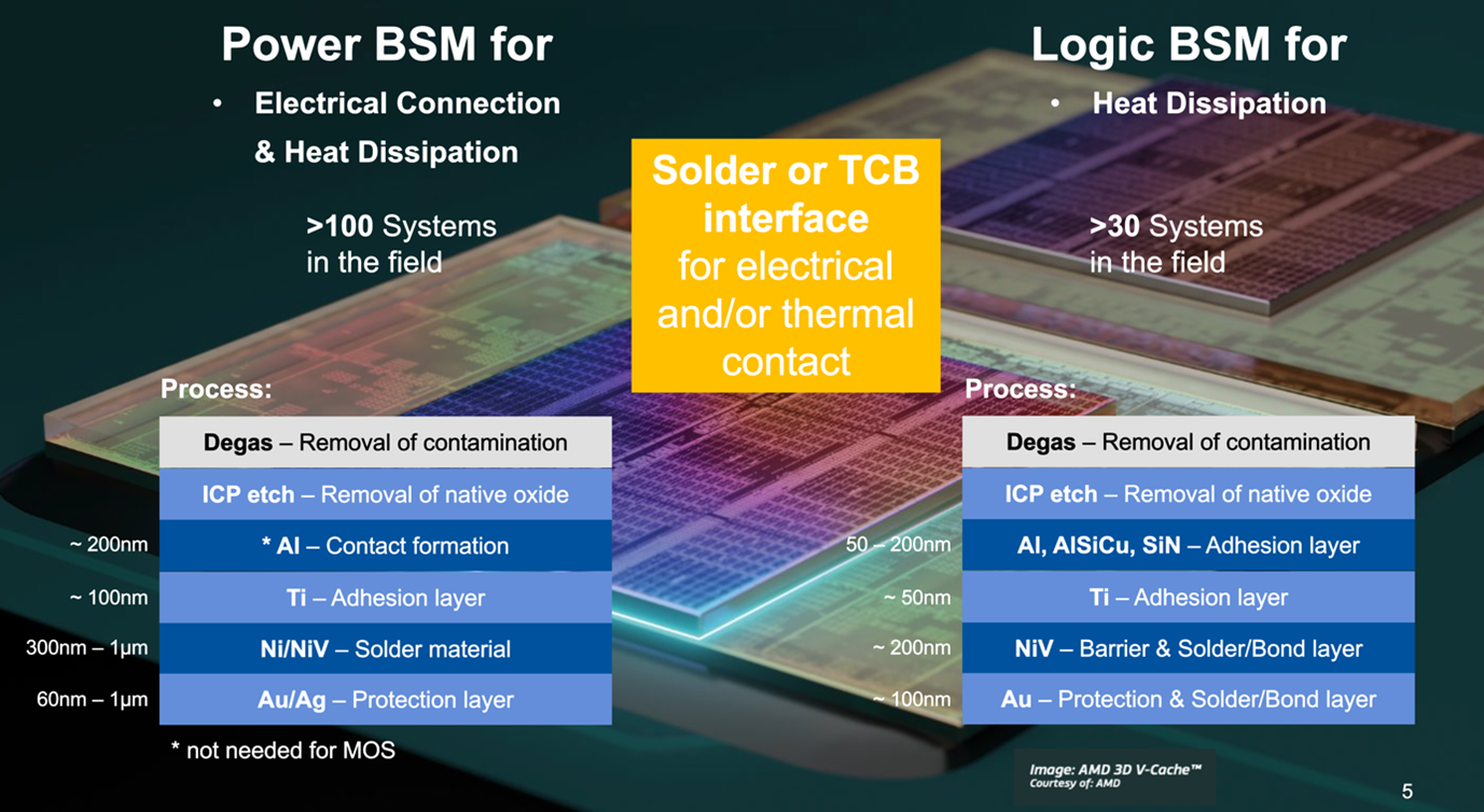
Backside Metallization for Heat Dissipation
High Performance Computing (HPC) is instrumental in various applications, including artificial intelligence, life sciences, and finance. To achieve optimal computing power, advanced system-on-chips (SOCs) or next-generation packaging technologies integrate processors, memory, and storage on die or package levels. However, effective thermal management poses a significant challenge in maximizing computing performance and power efficiency.
Evatec addresses this challenge through innovative thin film deposition techniques, particularly in backside metallization (BSM). Our BSM solutions facilitate uniform and reliable connections to cooling lids, essential for managing the heat generated by HPC packages. By depositing a solderable layer stack on the wafer's backside, we ensure excellent adhesion, solderability, and minimal film stress. These properties are crucial for meeting stringent thermal requirements and ensuring optimal performance and longevity of HPC systems.
Production Tools
The Evatec Tool Portfolio for Wafer Level Packaging
Choose from our platforms based on your substrate, process requirements, throughput, and factory integration needs.
Our experts are available to assist you in finding the right platform tailored to your specifications. Alternatively, click on the button to explore each platform in detail.
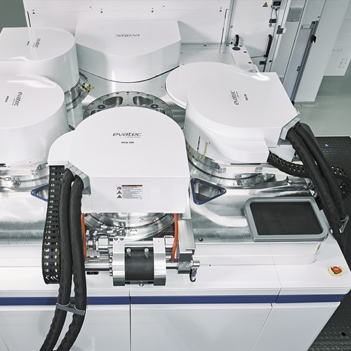
HEXAGON
Dedicated compact high volume production platform for wafer level applications like WLCSP and FOWLP on 200mm and 300mm offering high speed processing for the lowest cost of ownership in the market.
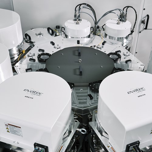
CLUSTERLINE® 300
Semiconductor industry standard 300mm cluster platform equipped with proprietary degas, arctic etch and metallization technology for WLCSP and FOWLP offering flexible manufacturing capability.
Read more about Wafer Level Packaging in our LAYERS magazine

Study of Cross-Contamination in Multi-Chamber PVD Systems
HEXAGON PVD systems are ideal for modern WLP applications, offering low and stable contact resistance at high throughput with minimal chamber-to-chamber cross-talk.
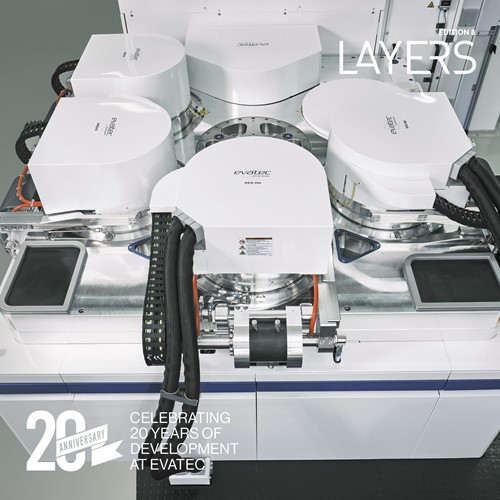
Productivity Boost and Optimum Rc Control in Wafer Level Packaging
The trend towards miniaturized electronic devices underscores the importance of low and stable contact resistance, with HEXAGON's high-throughput UBM / RDL technology validated through experimental work reported at ECTC.
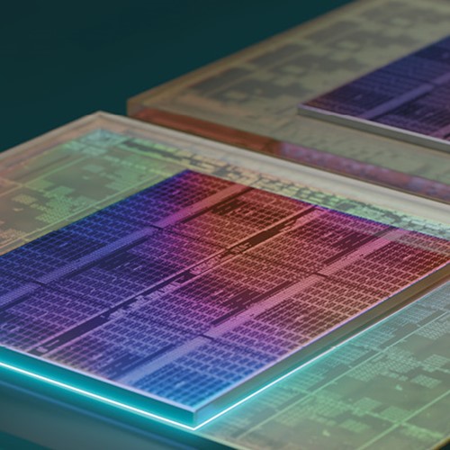
Chiplets and the new era of Advanced Packaging
As the industry enters the new era of heterogeneous integration, advanced packaging in the form of chiplets is becoming increasingly important. What is a Chiplet and what are the advantages?
