Welcome to the "Thin film Powerhouse". As a global leader in thin film technology we design and manufacture production systems for industry, and our customized engineering solutions support the equipment needed at the worlds' leading R&D institutions.
We would love to keep you updated with news of our company, products and market trends.
Who we are and what we do
Our technology has been shaping the world for over 70 years. Find out more about our company, our products and how Evatec thin films are everywhere in our daily lives.
Meet our management
Put a face to a name for our senior management team.
A global network of local offices
Find and contact your local sales and service office and see our network around the globe.
Get help from our company
We would love to hear from you. Complete the short contact form and we will be right back in touch.
Our company vision
Read about how we work together with our customers, employees and suppliers for the success of all.
Principles that guide our company
We respect those around us, support our community and save resources for the next generation. Find out more.
WE LOVE our Job and WE LOVE what we do! Would you also like to be part of an exciting future?
From our headquarters in Trübbach, we deliver high-tech solutions to customers all over the world. Have a look at our open positions in Switzerland or around the world and contact us to take the next step in your career.
Take a look at the latest opportunities
See how our employee's careers have developed and view the latest jobs available.
Apprentice opportunities
Folgende Lehrstellen bieten wir interessierten und lernwilligen Jugendlichen an.
We are focused on providing complete production solutions in our core markets of Advanced Packaging, Semiconductor, Optoelectronics and Photonics. Choose a market to find out how Evatec solutions can give you the lead.
Want to know more? Let us keep you updated in markets relevant to you.
Chip, wafer and panel level processing solutions
Learn about our innovative thin film solutions for wafer and panel level packaging applications such as WLCSP, FO WLP, FO PLP, 2.5D, 3D and advanced IC substrates.
Expertise in metallization and thin wafer processing
Benefit from Evatec's long experience in Power Device applications to increase your productivity, process stability and yield in volume production of MOSFETs, IGBTs, IGCTs, LDMOS, SiC and GaN Power Devices.
Thin films for sensing, actuating and magnetics
Learn more about Evatec technologies for metals, dielectrics and Advanced Functional Materials (Magnetics and Piezoelectrics) used in RF-MEMS, Sensors, Actuators, TFH and Soft-Magnetics in IVRs.
Expertise in RF filter technology using evaporation or sputter
Evatec leads in PVD production, offering advanced deposition processes for metals, contacts, piezoelectrics, and dielectrics. These enable technologies like RF filters, power amplifiers, HEMT on GaN, and IR devices. Our high-volume, high-performance solutions set the wireless market standard.
Solutions for LED and high performance optoelectronics
Read how Evatec's proven portfolio of platforms and PVD processes in daily production at the worlds’ leading (O)LED chip, micro LED and VCSEL manufacturers increase performance and drives down costs per lumen.
Optical coatings using advanced process control
From wafer level optics to 3D coatings, and from precision optics to decorative and functional coatings, read more about Evatec production solutions using Advanced Process Control (APC) technologies for the best repeatability and yield.
Bumping, Fan-Out Wafer-Level Packaging and Back-Side Metal Applications
Discover Evatec's Thin Film Solutions for Wafer-Level Packaging: Bumping (UBM), Fan-Out Wafer-Level Packaging (FO-WLP), and Back-Side Metal (BSM) Applications
Know-how in etch, evaporation, sputter and PECVD process technologies is at the very heart of our production platforms. Our Advanced Process Control (APC) technologies increase throughput, raise yields and lower cost of ownership.
Want to know more? We would be happy to send you updates on our technology.
A wealth of know-how in evaporation and sputter
Find out how Evatec's evaporation and sputter technology know-how can help you increase your yields and drive down your costs.
Plasma technology for coating modification or layer removal
From modification of sensitive coatings to high rate layer removal, read more about Evatec plasma source technology covering applications at wafer or panel level.
High quality coatings at low process temperatures
Learn about Evatec PECVD processes using PLASMABOX® technology and how they deliver optimum film quality by ensuring uniform heat distribution and very low levels of cross-contamination.
Increased precision and yield in thin film processes
See how Evatec's Advanced Process Control (APC) Technologies can help you increase precision and production yield for thin film processes.
We offer a range of batch, cluster and inline platform architectures equipped with evaporation, sputter, etch and PECVD source technologies according to your application, substrate format and throughput requirements. Benefit from over 50 years of process and production know-how. Choose an image to explore the hardware and process capabilities of each platform.
Want to know more? We would love to keep you updated with news of our products.
Evaporators from 0.5 to 2.0 metres with 50 years of process know-how
With over 2000 systems installed around the world find out why the BAK is the industry standard evaporator across semiconductor, optoelectronics and photonics.
A family of cluster platforms for wafer or panel processing up to 650mm
Benefit from the CLUSTERLINE® reputation of secure handling and precision processing on a range of platform sizes up to 650mm in applications across all Evatec core markets.
Your advantage for wafer level processes in Advanced Packaging
Process 300 or 200 mm substrates with highest throughput achieving lowest Rc in the industry. HEXAGON is the production platform that puts you ahead in UBM, RDL and Fanout.
Vertical sputter for metals, dielectrics and magnetic films
Compact design and flexibility make this vertical batch sputter tool for metals, dielectrics and magnetic films a cost effective choice for substrate sizes up to 200 x 230 mm.
Fully automated "inline" solutions for thin film production
From Touch Panels to EMI Shielding, Power Devices to Photovoltaics, SOLARIS® platforms are designed for "fully automated fabs". Choose from the S151 configured for substrates up to 8 inch diagonal or the S380 for substrates up to 15 inch diagonal.
Our global customer service team is here to help you through the whole life cycle of the tool from the moment the first installation is planned. Find out about some of the services we can offer.
Want to know more? We would love to keep you updated with news of our company and service solutions.
Evatec Customer Service - Get a quick overview of everything we offer
Find out more about our portfolio of services helping you get the most out of your Evatec tool.
Get access to original parts from our global warehouses
Fast and efficient - Get advice about the right spare parts services for you.
Remote or on site - you are never far away from help
Apart from urgent "tool down" support we offer services including planned maintenance and continuous improvement programmes. Find out more.
Extend the working life and capability of your Evatec production tool
Get the most from your Evatec tool by addressing obsolescence or adding new hardware and process capabilities. Learn how we can help you.
Training where and when you want it customized for you
Come to our facility in Switzerland, let our trainers come to you or use the latest "remote" technology. Our qualified instructors are ready to help you.
Read our latest news
Find all our news stories and updates on our products and technologies
Calendar of upcoming industry events
Get details of just some of the upcoming events where you can hear us speak or meet us at our exhibition booth
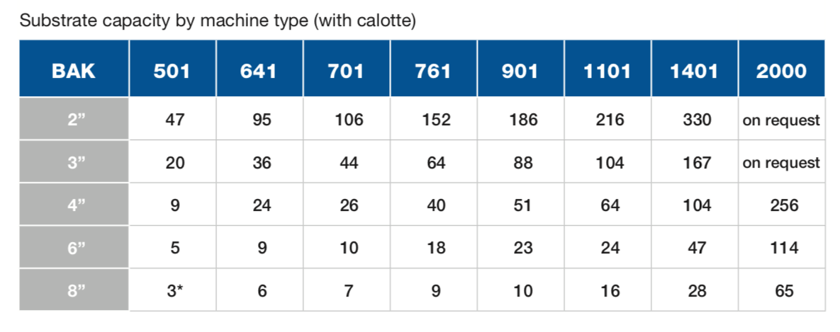
From the smallest to the biggest - here is a quick overview of substrate capacity according to system size