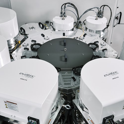
Leveraging Evatec know-how in both semiconductor and precision optics
Augmented & Virtual Reality
- Metals & dielectrics for waveguides
- Micro LED for displays & light engines
Emerging Automotive Display
- Proven LED thin film production solutions
- Micro LEDs / OLED on CMOS / Mini LED
More than 20 years of know-how in TCOs
- Customized hot and cold deposition processes
- Control of resistance, transmission, film roughness & grain structure
Cassette-to-Cassette processing
- 150, 200 and 300mm processing
- Low particles & secure handling for highest process yields
Experience Discrete LED / Laser Production solutions with Evatec
From cost effective process and production solutions for deposition of TCOs, metals and different types of DBR solutions to AlN buffer layer deposition, Evatec offers a broad range of standard and customized solutions to suit individual customers. Evatec addresses the requirements for downsized future LED dimensions including passivation / protection processes (SiO2 or SiN) with optimized film uniformities, reduced particle levels and further improved process and tool stability. Our solutions support manufacturing on form factors up to 12 inch and have been qualified by a number of fabs for the next generation Micro LED / display technology.
Just like in LED technology Evatec can offer know-how across a number of processes in the manufacturing chain for VCSEL and EEL technologies. Evatec already has more than 15 years know-how in delivering manufacturing solutions for DBRs, TCOs, metals and passivation layers in LED applications. That know-how can be leveraged to develop tailored thin film processes for VCSEL and EEL together with customers too.
LED Devices (Mini-, MicroLED)
In the realm of LED production, factors such as cost efficiency and technical specifications like light output (LOP) and forward voltage (Vf) have traditionally held sway. However, with the advent of MicroLED technology, new challenges have taken center stage, particularly in this nascent phase:
- The significantly thinner structures of MicroLEDs underscore the critical importance of achieving uniform thickness across wafers and ensuring repeatability from batch to batch.
- These structures, often two orders of magnitude smaller, demand even tighter control over particles to meet the stringent device yield requirements.
To meet the exacting standards of MicroLED fabrication, the adoption of automated load lock systems is imperative. These systems maintain process chambers under continuous vacuum, ensuring optimal process stability and minimizing particle contamination. Furthermore, eliminating manual handling at the front-end reduces errors and enables precise tracking of each wafer throughout production.
Similar to traditional LED manufacturing, a holistic understanding of the entire LED process chain is paramount. Leveraging our extensive experience and close collaboration with clients, we recognize that optimal device performance and yield stem from fine-tuning individual processes as part of a comprehensive package. Here's a brief overview of the processes where we excel in adding value for our customers:
Key Processes for Enhanced LED Manufacturing
- check Transparent Conductive Oxides (TCOs) like ITO and AZO
- check P contacts such as Al, Ti, Ni, Pt, and Au
- check N contacts including Al, Ti, Ni, Pt, and Au
- check Reflection layers, encompassing Distributed Bragg Reflectors (DBRs), metals, or hybrid DBRs
- check Capping layers, comprising metals or SiO2
- check Finalization processes like low-stress passivation
In the early stages of MicroLED technology development, various manufacturing approaches, including "mass transfer" and "monolithic," are being explored. Evatec's expertise in TCOs (ITO, AZO), Mirrors (DBR, Ag), and Metals (Ni, Ti, Pt, Au, WTi) enables us to support both methods with the deposition of high-transmission films across the entire visible spectrum.
You can read more about Evatec production platform and processes for MicroLED in LAYERS 8.

Pioneering the future of LED and laser technology with precision and innovation.
Laser Diodes (VCSEL, EEL)
Laser diodes, encompassing Vertical-Cavity Surface-Emitting Lasers (VCSEL) and Edge-Emitting Lasers (EEL), play a pivotal role in advancing 3D sensing technology. While applications like face recognition in mobile phones have already embraced 3D sensing, emerging sectors such as Autonomous Driving necessitate tailored solutions based on time-of-flight (TOF) with Near-Infrared (NIR) VCSEL and EEL technologies. Additionally, shortwave VCSELs and blue VCSELs are garnering attention for their potential in diverse applications like data communications, 3D printing, chip-sized atomic clocks, and high-brightness light sources.
Similar to our expertise in LED technology, Evatec boasts a wealth of knowledge across various processes in the manufacturing chain for VCSEL and EEL technologies. With over 15 years of experience in providing manufacturing solutions for Distributed Bragg Reflectors (DBRs), Transparent Conductive Oxides (TCOs), metals, and passivation layers in LED applications, we possess the expertise to tailor thin film processes for VCSEL and EEL in collaboration with our customers.
Unlike LEDs, where photons typically undergo single reflection within the active region, VCSEL cavities facilitate multiple reflections. Therefore, achieving high reflectivities on both front and back sides of DBRs is crucial to mitigate light output losses.
Sputtered DBR layers offer several performance advantages over traditional epitaxial layers, particularly in the blue domain, including:
- check Higher peak reflectance for improved light output
- check Wider stop band for larger wavelength range
- check Lower spectral shift for improved yield
- check Thinner stack structure for less surface stress
- check Lower total resistance for increased efficiency
You can read more about Evatec production platforms and processes for VCSEL and EEL, including new processes for enhanced side wall coverage enabling a wafer level optics approach to EEL manufacturing, in the LAYERS articles below.
Production Tools
The Evatec Tool Portfolio for Descrete LED / Laser
At Evatec, we provide a comprehensive range of production tools tailored for Discrete LED/Laser applications. Our portfolio includes cutting-edge evaporation, sputtering, and etching technologies available on various platforms, including batch, cluster, or fully automated inline systems.
Our experts are on hand to help you find the right platforms according to your process requirements, throughput and factory integration requirements. Alternatively, click on the buttons to read more about each platform.

BAK Family
Additional options are available for fully automated cassette to cassette production on 6 or 8 inch. Industry standard evaporator platforms for metals deposition and “lift off” processes.

CLUSTERLINE® 200
An optoelectronics workhorse at leading LED and Micro LED Display manufacturers. Production proven for deposition processes including metals, TCOs and DBRs.

CLUSTERLINE® 300
Semiconductor industry standard cluster tool offering high uniformity deposition and etch capability on 300mm substrates and know-how for applications including OLED on CMOS.

LLS EVO II
Vertical batch sputter platform with long market pedigree the guaranteeing lowest cost of ownership especially for metal deposition.
Read more about Discrete LED / Laser in our LAYERS magazine

Side Wall Coverage
Evatec explains why device side wall coverage is becoming important for thin film processes in Optoelectronic applications like Micro LED.

Hybrid DBRs
Discover Evatec's latest Micro LED technology developments, offering lower costs and more compact structures to drive mass market growth.

Edge Emitting Lasers
Explore production solutions for the antireflection and high reflectivity coatings needed in emerging applications for Edge Emitting Lasers (EELs).
